
Preparation of Core Raw Materials
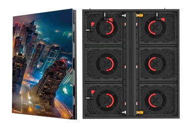
Selection of stable, high-luminous-efficiency LED chips paired with PCBs offering high thermal conductivity and heat dissipation, alongside high-precision driver ICs and electronic components such as resistors and capacitors.
Indoor display brightness is controlled within the 500–1500 cd/m² range to prevent excessive glare.
Core Module Manufacturing Processes
SMD Process: LED chips are packaged into individual beads and then mounted onto the circuit board; this is a mature, cost-effective technology and the mainstream choice for indoor applications.
COB Process: Chips are packaged directly onto the PCB, eliminating the need for individual bead housings; this offers superior protection and heat dissipation, enables finer pixel pitches, and is commonly used in high-end command centers and conference rooms.
Advanced Processes: GOB and VOB are upgraded versions of SMD that utilize transparent or nano-adhesives for protective coating, significantly enhancing resistance to moisture, dust, and physical impact.
Full Screen Assembly and Calibration
Following die bonding, wire bonding, and encapsulation curing, modules are assembled by installing housings and connecting ribbon cables and power supplies, ensuring correct polarity.
During module splicing, uniform gaps are maintained, and pixel-by-pixel calibration technology is employed to eliminate pixel discrepancies, achieving brightness uniformity of over 90%.